
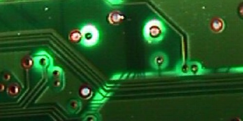
Figure 1. Circuit Board With Common Design Flaw
Abstract: Common circuit
design flaws at the board and system level cause many operational
problems. Some of these flaws were understood and fixed years ago, yet
still show up in designs. A few
common problems of this type are discussed and examples given.
Discussion: In my consulting
work, I see a lot of operational problems in systems that are caused by
common circuit design flaws. In this Technical Tidbit, several of these
flaws are discussed and examples are shown. A thread that runs
through many of these examples, and my consulting work, are problems
caused by attempting to separate "grounds" into different regions with
"single point" connections between them. An example might be to
separate a printed wiring board, PWB, ground plane into analog and
digital areas.
There are a few relatively rare cases where grounds must be split apart, but when this is done a great deal of care must be taken to avoid problems. In most cases I have seen, separating grounds caused operational problems in a system. Grounds should be separated only if absolutely necessary and with concrete evidence (preferably based upon measurements) that doing so is required. Application notes in device manuals sometimes give incorrect advice on this topic.
So, let's start with my favorite problem, ground plane breaks on a PWB.
1. Ground plane breaks: Figure 1 above shows a small section of a PWB with a light shining through the board so breaks in the power/ground planes can be easily seen. Notice paths crossing a break in the power/ground planes at random. There are many effects of doing this covered in the linked articles at the bottom of this page. The situation is illustrated in Figure 2.
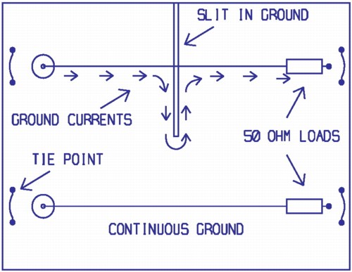
Figure 2. Drawing of Test Board With Slotted Ground
Figure 2 shows a layout diagram of a small test board, about 10 cm by 15 cm, that is used in a number of my Technical Tidbits. The bottom signal path is over a continuous ground plane whereas the top path crosses a 5 cm slot in the solid copper planes. The board has two planes with an identical break in each. The plane on the back side of the board is not used but is shorted to the top plane by the BNC connectors on the left end of each path.
All signals form a loop, from source to load and back again and it is the "back again" that often leads to problems. In this case, the returning current for the bottom path forms a long (the length of the signal path) but very thin loop, just a few mils in height. However, for the upper path, the returning current to the source must pass around the end of the slot in the ground plane and in doing so forms a substantial loop. The many bad effects of this loop are described in the Technical Tidbits linked at the bottom of the page and include slowed risetime, increased crosstalk to other paths, EMI emissions, and susceptibility to ESD and radiated RF fields. Figures 3 and 4 show two more examples of paths crossing plane breaks that cut all the way through the board. It is amazing to me that such features still show up in board designs today.
There are a few relatively rare cases where grounds must be split apart, but when this is done a great deal of care must be taken to avoid problems. In most cases I have seen, separating grounds caused operational problems in a system. Grounds should be separated only if absolutely necessary and with concrete evidence (preferably based upon measurements) that doing so is required. Application notes in device manuals sometimes give incorrect advice on this topic.
So, let's start with my favorite problem, ground plane breaks on a PWB.
1. Ground plane breaks: Figure 1 above shows a small section of a PWB with a light shining through the board so breaks in the power/ground planes can be easily seen. Notice paths crossing a break in the power/ground planes at random. There are many effects of doing this covered in the linked articles at the bottom of this page. The situation is illustrated in Figure 2.
Figure 2. Drawing of Test Board With Slotted Ground
Figure 2 shows a layout diagram of a small test board, about 10 cm by 15 cm, that is used in a number of my Technical Tidbits. The bottom signal path is over a continuous ground plane whereas the top path crosses a 5 cm slot in the solid copper planes. The board has two planes with an identical break in each. The plane on the back side of the board is not used but is shorted to the top plane by the BNC connectors on the left end of each path.
All signals form a loop, from source to load and back again and it is the "back again" that often leads to problems. In this case, the returning current for the bottom path forms a long (the length of the signal path) but very thin loop, just a few mils in height. However, for the upper path, the returning current to the source must pass around the end of the slot in the ground plane and in doing so forms a substantial loop. The many bad effects of this loop are described in the Technical Tidbits linked at the bottom of the page and include slowed risetime, increased crosstalk to other paths, EMI emissions, and susceptibility to ESD and radiated RF fields. Figures 3 and 4 show two more examples of paths crossing plane breaks that cut all the way through the board. It is amazing to me that such features still show up in board designs today.
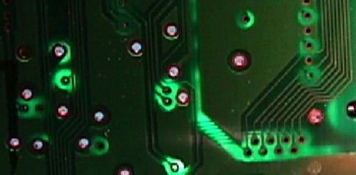
Figure 3. Another Circuit Board Example of Signals Crossing Plane Breaks
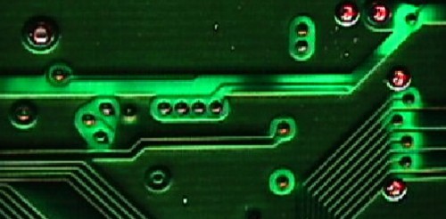
Figure 4. Third Circuit Board Example of Signals Crossing Plane Breaks
In Figure 4 there are two interesting features. The smaller one is the vertical field of vias near the lower right corner of the picture. The cutouts in the power and ground planes for these vias are large enough to overlap and form a slot in the planes. If there was enough room to get the horizontal signals in-between the vias, then there is a good chance that paths could also pass between the vias on the power and ground layers to slice up the slot into smaller pieces. Although I can't tell if this was done on this board, I doubt those paths were added.
The larger feature to note in Figure 4 is the horizontal slot between the digital and analog areas of the board (complete with a few signals paths in the break!). The designers thought the break was necessary to avoid digital noise getting into sensitive small signal analog circuits. Needless to say this board had a lot of problems including excessive emissions. When all plane breaks were filled in, the board worked perfectly (no analog problems) and emissions were reduced.
2. Single point grounding of printed wiring boards: This feature of system design is more common than I would expect and often causes operational problems. Figure 5 shows a board from an old disk drive mounted on a copper clad board for test purposes. The results of injecting ESD at the lower left are described in my May 2002 Technical Tidbit and they are not what many engineers expect. Single point grounding of the board (the upper right connection was used in the test) resulted in a lot of current ringing at about 200 MHz due to the ESD hit. The board and copper plane formed a nice parallel plate capacitor and with the single connection point inductance formed a high Q tuned circuit at 200 MHz, not a desirable thing to do. Adding the other three connections to the copper plane raised the resonant frequency to about 500 MHz and the upper right corner connection became very quiet compared to the case where it was the only connection.
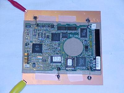
Figure 5. A Disk Drive Board Mounted Over a Copper Plane
Figure 6 shows a related example that occurs in a lot of the equipment I see. All the boards in a system are isolated from chassis except for one at a single point. This is even worst than the case shown in Figure 5. ESD to one board travels through all boards on the way to the chassis with the current path modified the the capacitance between the boards and the chassis. This case is discussed in greater detain in my March 2007 Technical Tidbit. It is a very rare case where this system architecture is really necessary. In every case I have seen, a better alternative was available to meet system requirements. One example would be the use of an isolated interface for those connections that really need isolation and then connect the boards securely to the chassis in many places. In rare cases, one of the chassis connections may cause a problem, and when it does, treat that case as an exception and analyze what is happening. It is a lot easier to remove an existing connection than to add a new one to a design.
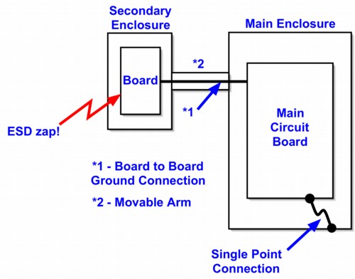
Figure 6. Circuit Boards Isolated From Chassis Ground Except at a Single Point
3. Processor reset lead routing:This one occurs too often for comfort. I have seen processor reset leads routed all over a processor board, bad enough in itself, and then extended to a noisy I/O board as well! Recently, I worked on a case where a 10 cm reset trace on a four layer board caused the circuit to reset in response to an ESD event across the room. The fix was to filter the reset with an RC filter near the processor. Remember, when it comes to ESD, lead lengths of one cm can be too long, for example in the RC filter example.
5. Off-spec use of protection components: My final example is using components that are not specified for the application, My August 2005 Technical Tidbit describes an example of a lighting TVS protection device used for ESD protection. Small surface mount and leaded inductors have their characteristics specified at a few MHz and then we use them at hundreds of MHz. My May 2000 Technical Tidbit shows a method of evaluating small inductors to mitigate the effects of ESD. In that article, it was shown that the best effect was obtained by placing a smaller inductor in series with a larger one.

Figure 4. Third Circuit Board Example of Signals Crossing Plane Breaks
In Figure 4 there are two interesting features. The smaller one is the vertical field of vias near the lower right corner of the picture. The cutouts in the power and ground planes for these vias are large enough to overlap and form a slot in the planes. If there was enough room to get the horizontal signals in-between the vias, then there is a good chance that paths could also pass between the vias on the power and ground layers to slice up the slot into smaller pieces. Although I can't tell if this was done on this board, I doubt those paths were added.
The larger feature to note in Figure 4 is the horizontal slot between the digital and analog areas of the board (complete with a few signals paths in the break!). The designers thought the break was necessary to avoid digital noise getting into sensitive small signal analog circuits. Needless to say this board had a lot of problems including excessive emissions. When all plane breaks were filled in, the board worked perfectly (no analog problems) and emissions were reduced.
2. Single point grounding of printed wiring boards: This feature of system design is more common than I would expect and often causes operational problems. Figure 5 shows a board from an old disk drive mounted on a copper clad board for test purposes. The results of injecting ESD at the lower left are described in my May 2002 Technical Tidbit and they are not what many engineers expect. Single point grounding of the board (the upper right connection was used in the test) resulted in a lot of current ringing at about 200 MHz due to the ESD hit. The board and copper plane formed a nice parallel plate capacitor and with the single connection point inductance formed a high Q tuned circuit at 200 MHz, not a desirable thing to do. Adding the other three connections to the copper plane raised the resonant frequency to about 500 MHz and the upper right corner connection became very quiet compared to the case where it was the only connection.
Figure 5. A Disk Drive Board Mounted Over a Copper Plane
Figure 6 shows a related example that occurs in a lot of the equipment I see. All the boards in a system are isolated from chassis except for one at a single point. This is even worst than the case shown in Figure 5. ESD to one board travels through all boards on the way to the chassis with the current path modified the the capacitance between the boards and the chassis. This case is discussed in greater detain in my March 2007 Technical Tidbit. It is a very rare case where this system architecture is really necessary. In every case I have seen, a better alternative was available to meet system requirements. One example would be the use of an isolated interface for those connections that really need isolation and then connect the boards securely to the chassis in many places. In rare cases, one of the chassis connections may cause a problem, and when it does, treat that case as an exception and analyze what is happening. It is a lot easier to remove an existing connection than to add a new one to a design.
Figure 6. Circuit Boards Isolated From Chassis Ground Except at a Single Point
3. Processor reset lead routing:This one occurs too often for comfort. I have seen processor reset leads routed all over a processor board, bad enough in itself, and then extended to a noisy I/O board as well! Recently, I worked on a case where a 10 cm reset trace on a four layer board caused the circuit to reset in response to an ESD event across the room. The fix was to filter the reset with an RC filter near the processor. Remember, when it comes to ESD, lead lengths of one cm can be too long, for example in the RC filter example.
4. Ground bounce induced emissions problems:
Most chip packages with large chips within, such as a processor, have
ground bounce on the chip relative to the board of tens of millivolts.
This is enough to make all circuit traces on
the board leaving the IC package RF hot to the point of causing excessive
emissions. The typical scenario is where a processor is driving an LED.
Being a dc signal, the LED path is routed with no regard to high
frequency effects, such as crossing ground plane breaks. However, the IC
package ground bounce makes the LED signal hot enough to radiate and
cause emissions failures during compliance testing. Don't do this! Buffering or filtering the LED signal will solve the problem.
5. Off-spec use of protection components: My final example is using components that are not specified for the application, My August 2005 Technical Tidbit describes an example of a lighting TVS protection device used for ESD protection. Small surface mount and leaded inductors have their characteristics specified at a few MHz and then we use them at hundreds of MHz. My May 2000 Technical Tidbit shows a method of evaluating small inductors to mitigate the effects of ESD. In that article, it was shown that the best effect was obtained by placing a smaller inductor in series with a larger one.
Figure 7. TVS Protection Device
Summary:
Some of the most frequent circuit design flaws I see in my consulting
work have been described. In some cases, the problem was understood and
solved years ago and yet still shows up in current circuit designs.
Links to Technical Tidbit articles on this website with more
information are provided.
Additional article on this website related to this topic is:
- May 2000, Measuring Inductor Performance
- May 2002, Printed Wiring Board Coupling to a Nearby Metal Plane, Part 2: ESD Immunity
- December 2002, Crossing Ground Plane Breaks, A Source of Crosstalk
- January 2003, Crossing Ground Plane Breaks - Part 2, Tracing Current Paths
- February 2003, Crossing Ground Plane Breaks - Part 3, Immunity to Radiated EMI
- January 2005, Crossing Ground Plane Breaks - Part 4, Risetime Effects on Signals
- February 2005, Crossing Ground Plane Breaks - Part 5, Common Mode Currents and Emissions
- August 2005, Off-spec Use of Protection Components
- March 2007, Isolating Board and Chassis Grounds - A Potential Problem (An ESD Example)
Click here for a description of my latest seminar to be available soon titled:
EMC
Lab Techniques for Designers
(How to find EMC problems and have some confidence your system will pass EMC testing while it is still in your lab).
(How to find EMC problems and have some confidence your system will pass EMC testing while it is still in your lab).
 |
Check out my podcast containing mp3 format short tutorials, tech news and more! Just click on the microphone to see the listing
of free
audio programs. Content is added every week on technical topics so check back frequently. |
Home