Printed Wiring Board Coupling to a Nearby Metal Plane
Part 2: ESD Immunity
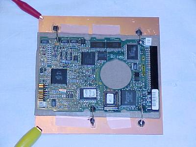
Figure 1. Test Board Mounted Close to a Metal Plane

Address: P. O. Box 1457, Los Gatos,
CA 95031
TEL:
800-323-3956/408-356-4186
FAX:
408-358-3799
Mobile: 408-858-4528
URL:
www.dsmith.org
Email: doug@dsmith.org
Figure 1. Test Board Mounted Close to a Metal Plane
The April 2002 Technical Tidbit, Printed Wiring Board Coupling to a Nearby Metal Plane, presented data generated by the continuous signal from an oscillator. This month, a circuit board from a disk drive is used to show how board coupling to a nearby metal plane can effect the results of transients, such as ESD, applied to a system. The result, as you will see, is quite surprising.
Figure 1 shows the circuit board mounted above a ground plane (copper clad board) using a cardboard spacer between the circuit board and the plane to achieve a 3 mm spacing. The separation distance of 3 mm is similar to the the distance between some circuit boards and a nearby chassis. A 1000 volt contact discharge was applied to the plane by the yellow clip at the lower left of the picture. The red lead on the upper left was a two meter earth ground lead to drain away the static charge after the ESD event.
ESD was applied to the metal plane under two conditions. First with only one ground bond between the board and the plane, the one at the upper right of Figure 1, and secondly with all four ground bonds present. An approximately 1 cm by 2 cm square shielded magnetic field probe (link document is ~600K) was used to measure the voltage drop across the ground bonding leads under both grounding conditions. The measurement was made as shown in Figure 2. I estimate that the m(di/di) voltage output of the loop into 50 Ohms is about 1/6 of the voltage across the short bonding wire since the loop is parallel to the wire for about 1/2 its length. And, the coupled voltage into the loop used would be about 1/3 of the voltage across the wire adjacent to the loop.
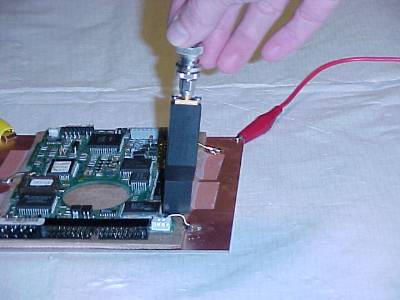
Figure 2. Current in Wire Connecting Output of Oscillator to Plane
(oscillator off plane)
Figure 3 shows the loop output when only one ground bond is present (upper right of Figure 1 and the loop is held next to that wire as shown in Figure 2. A 7 Volt P-P waveform with 200 MHz ringing frequency resulted. This means that the voltage drop across the wire is on the order of 6x7 or about 40 Volts! Remember that the ESD was applied to the opposite end of the plane or "chassis" from the "only" connection between the metal plane and the PWB. Obviously the board is strongly coupled to the plane. Imagine what would happen if the ground bond was actually a connector with a ground pin (or several ground pins) that connected a daughter board to a mother board with no other connections between the boards. Corruption of the signals is a good possibility.
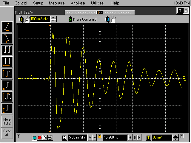
Figure 3. Loop Output at Single Ground Bond (upper right of Figure
1).
Figure 4 shows the loop output when positioned the same as before over the bonding wire in the upper right of Figure 1, but with all four ground bonds present. The difference is dramatic, with an observed loop voltage of only about 300 mV. This was about the same amplitude that resulted when the loop was held about 15 cm above the circuit board (a "null" experiment to check if the signal was due to currents in the bonding wire). The value of 300 mV is likely due to radiation directly into the loop from the ESD simulator and thus may not be due to current flowing in the bonding wire.
One of the reasons cited for using a single board ground is to keep ESD currents from flowing onto and off of the board. As can be seen, the board coupling to the underlying metal plane is so strong the currents will flow anyway and multiple connections can even reduce the board currents as shown in Figure 4.
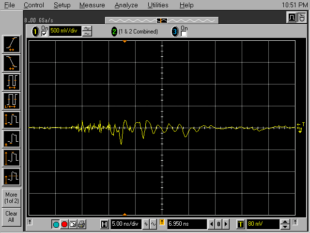
Figure 4. Loop Output at Ground Bond (upper right of Figure 1) With
Four Ground Bonds Present
One must still use judgment in the placement of critical circuits on a board though. Figure 5 shows the loop output when it was positioned on the ground bond wire at the upper left of Figure 1, with all four ground bonds present. For this case, the output reached a peak of about 3 Volts, but without the high-Q ringing shown in Figure 1. The ground bond is very close to the attachment point of the red ground lead to the metal plane and one might expect a concentration of ESD currents there. Such currents flowing on the bonding lead spread out on the board and can potentially cause problems. This is not to say one should minimize ground bonds (remember Figure 3), but just pay attention to where sensitive circuitry is located on the board. The more ground bonds used, the less current any one has to carry and positioning may be less of an issue. For this example, it might be a good idea to keep sensitive circuits away from the area of the board near the ground bond at the upper left of Figure 1.
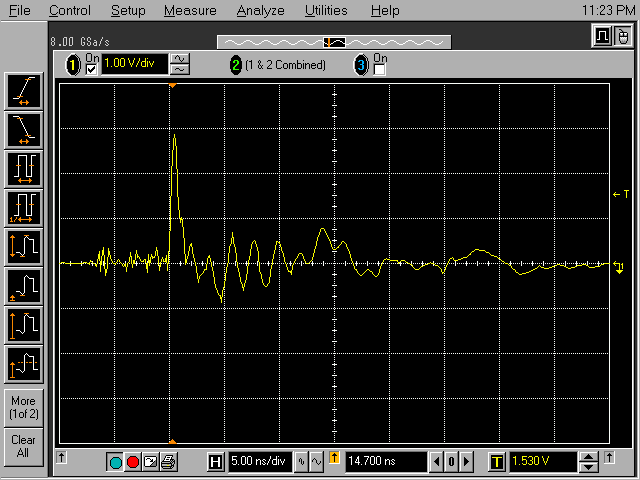
Figure 5. Loop Output at Ground Bond (upper left of Figure 1) With
Four Ground Bonds Present
A good design practice might to use multiple ground bonds (if the system architecture allows for it) and keep sensitive circuitry away from board grounds near sources of ESD current. During development, one could mount a blank plane to simulate a board in the system enclosure and measure the ESD voltage drops across the board ground bonds using a shielded loop while ESD is applied to the enclosure at expected places. Factor the results of this experiment into the board layout to minimize problems. Doing such an experiment early in system design is a good way to reduce risk. If one discovers that there are sensitive circuits near a concentration of ESD current, either add more ground bonds in the vicinity to minimize what any one bond carries or move sensitive circuitry away from the danger area.
Other articles on this website containing information on magnetic field probes or the effects of metal planes include:
Much more information on this effect and issues discussed in the other Technical Tidbits is presented in my public and private seminars.