Abstract: E-field probes can
be very useful in EMC settings where measurements are usually made in
the far field [1][2]. E-field probes behave quite differently in the
near field and when used for troubleshooting circuits, they arre usually in
the near field. E-field probes, used in the near field, can be useful
for troubleshooting designs by concentrating the field to a small
portion of a PCB or system. A useful, easy to build, near field E-field
probe is describes and its performance illustrated with data.
Figure 1 shows
the
completed easy to build E-field probe. In Figure 2, the main components
of the probe are shown: a BNC barrel and a carpet tack. The tack is
selected to have the nail portion the right size to fit the center pin
of the BNC barrel. A carpet tack is better than a thumb tack
because the nail section is longer and of the right diameter for the
BNC barrel. If the tack is painted like the one in Figure 2, sandpaper
or a file should be used to remove the paint from the nail section so
it makes good contact with the BNC.
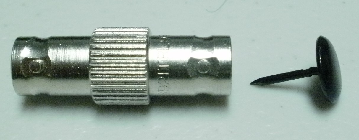
Figure 2. BNC Barrel and Carpet Tack Used to Make the E-Field Probe
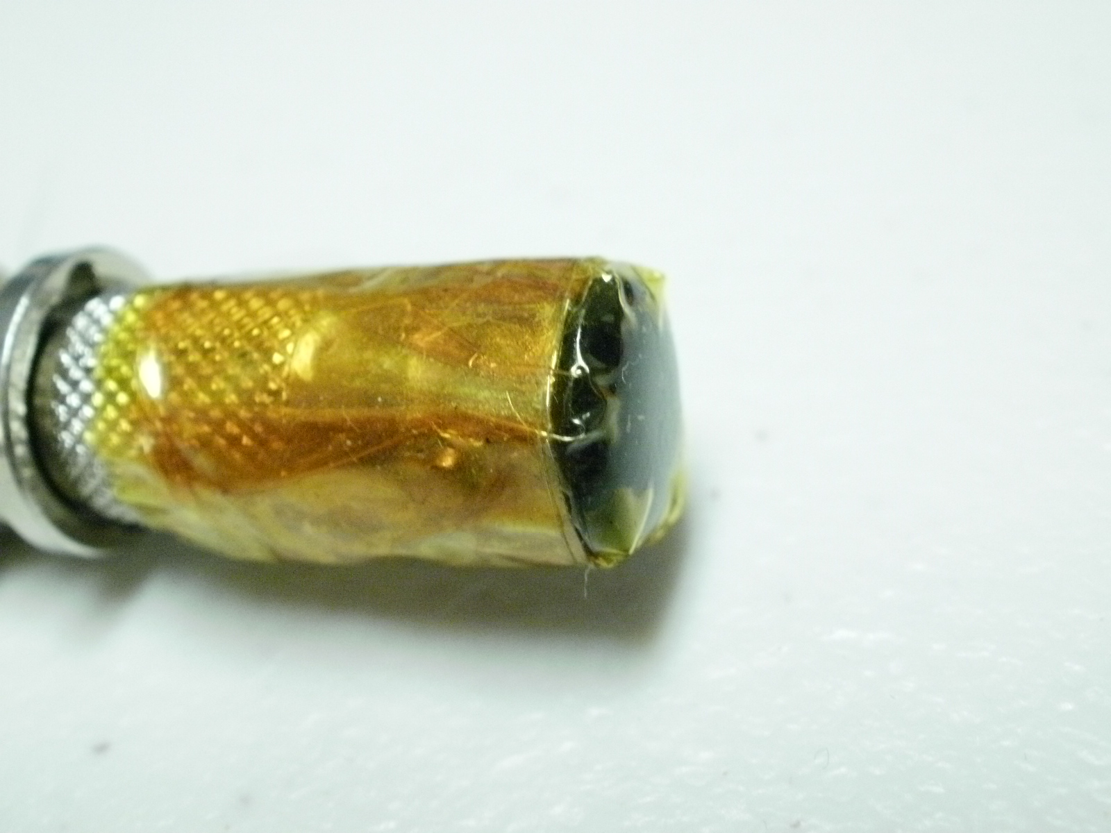
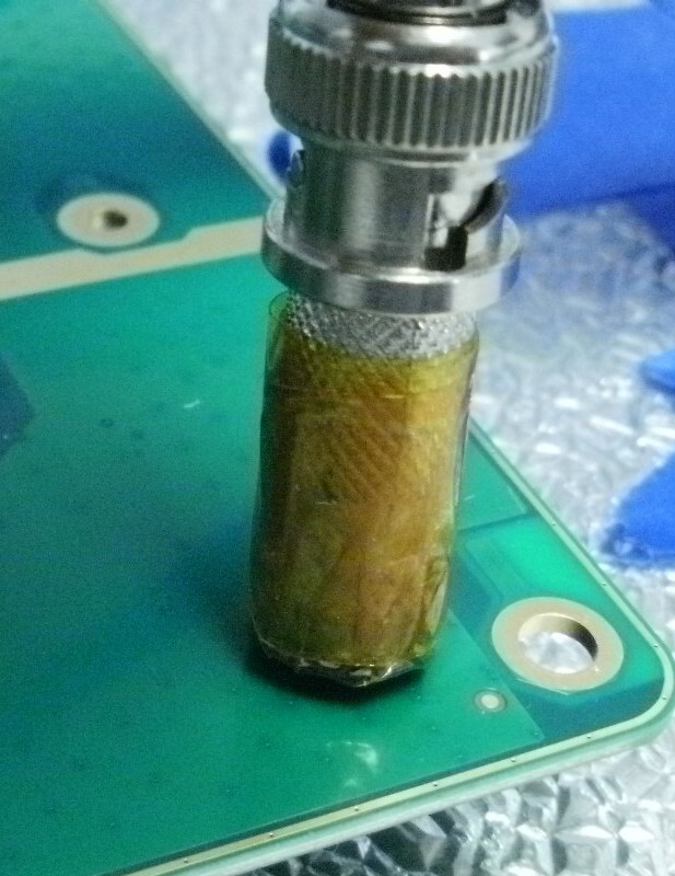
Next the end of the BNC barrel is covered with Kapton tape (the stuff
that holds Silicon Valley together) which is folded down over the
outside of the barrel. The tape should be wide enough to completely
cover the end of the BNC barrel and some extra. The tack is inserted through the tape
into the BNC. A this point, the head of the tack is resting on the
tape, insulated from the BNC barrel. Then a second piece of Kapton tape
is applied over the track to insulate it. This piece of tape should be
at 90 degrees to the first piece on the outside of the BNC barrel. Then
a third piece of tape should be added around the circumference of the
BNC to hold the other two pieces down. The probe should look like the
one in Figure 3 at this point.
Figure 3. Probe Covered in Kapton Tape
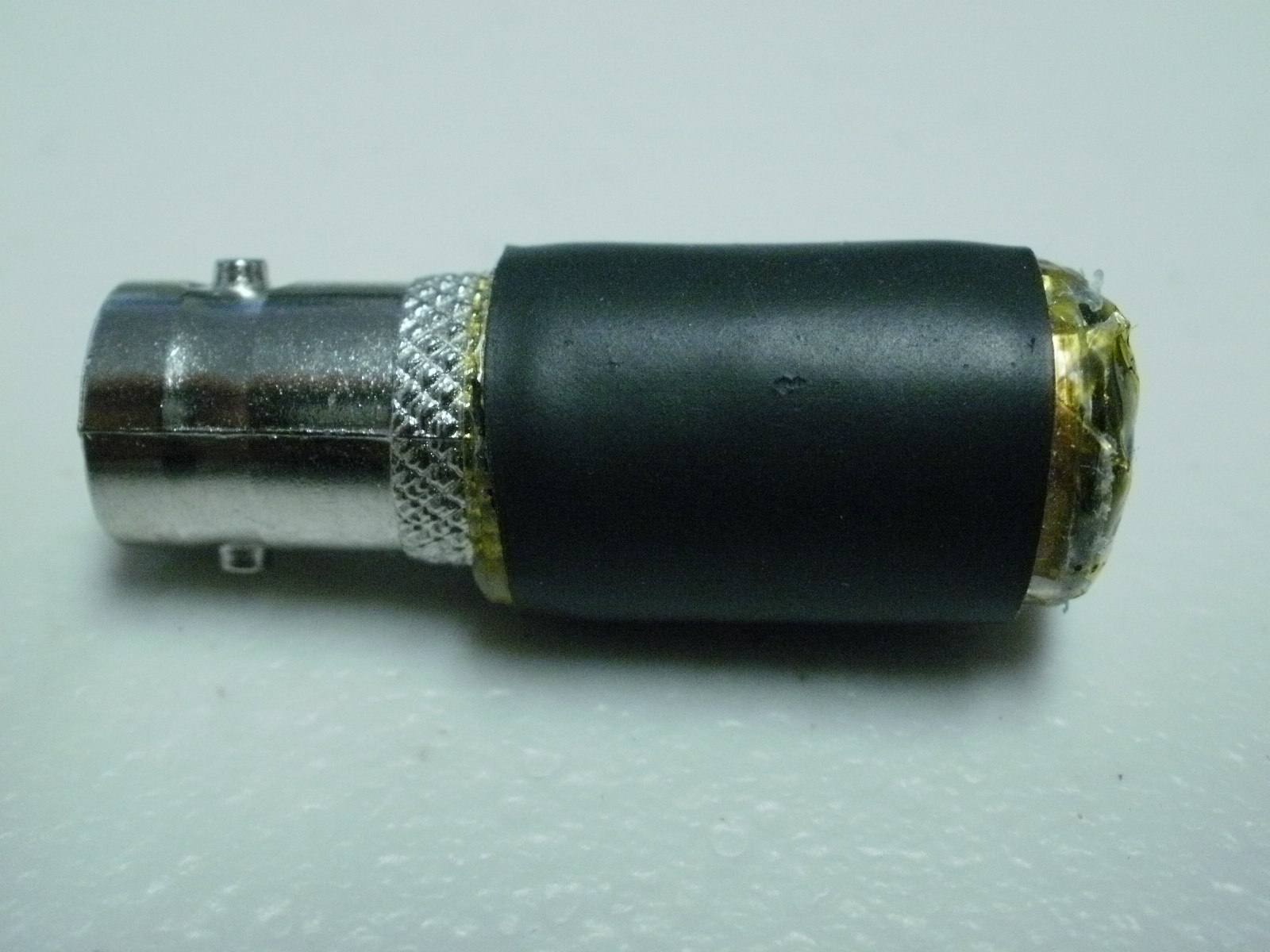
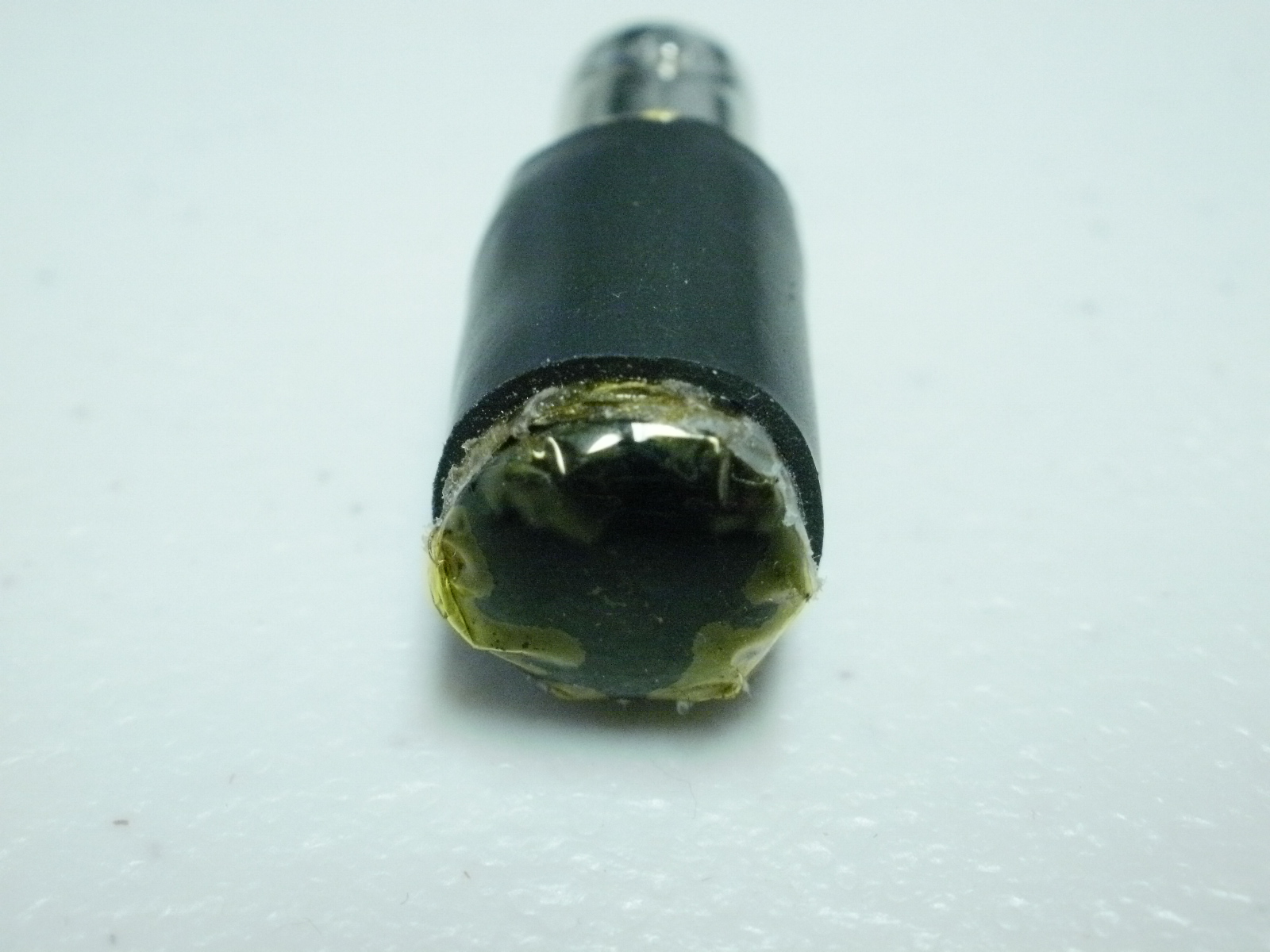
A final touch of heat shrink tubing can be added as shown in Figure 4
for a nice look and to insure the layers of tape are held down. The
tubing also serves to make a grip for holding the probe securely.
Figure 4. Heat Shrink Tubing Used to Finish the Probe
Figure 5 shows how the probe is used. It is generally held at right
angles to a PCB and fed from a high voltage pulse generator to inject
capacitively coupled current locally into the PCB at one spot.
Figure 5. Using the E-Field Probe to Scan a PCB
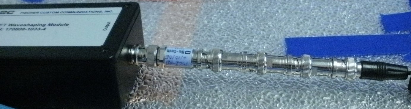
Figure 6 shows a Fischer Custom Communications "EFT" high voltage pulser
with external attenuators feeding the E-field probe. The pulse shape
has a fast rise, slow fall, and is designed not to burn out most 2 Watt
attenuators. For the measurements below, a single 6 dB attenuator was
used to keep the scope plot on the screen.
Figure 6. Using a Fischer Custom Communications "EFT" High Voltrage Pulser and Attenuators to Drive the E-Field Probe
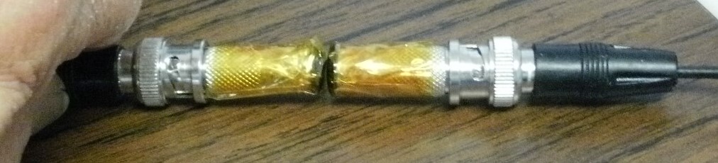
With the pulser running, the setup shown in Figure 7 was used to
measure the injected current from one probe to a second probe with a 50
Ohm termination at the scope input. The result gives an idea what might
be injected into a PCB. The result is shown in Figure 8. The waveshape
will vary considerably with the length of the cables and nearby objects
as the outside of the coax shields are in the current path. Injected
current into the receiving probe is matched with a current flowing on
the cable shield in the opposite direction (traveling out of the cable
shield and along the outside of the coax shield away from the probe.
Injected E-fields effects on a PCB are usually less contained in area
than H-fields that form local current loops in a ground plane or
signals injected into signal traces. H-field injection is not
particularly sensitive to surrounding objects like E-field injection
is.[3]
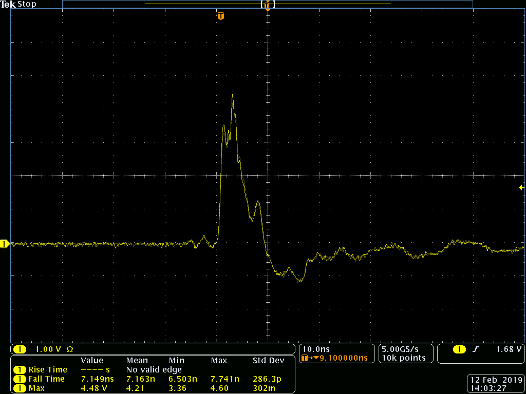
Figure 8 shows a peak voltage injected into the second probe of about 8
Volts, a significant amount. The pulse width is about 5 ns, the risetime
of the pulser. There is a much smaller negative pulse corresponding to
the longer fall time of the pulser, about 25-30 ns.
Figure 7. Coupling Two E-Field Probes to Measure Injected Voltage Into a 50 Ohm Load
Figure 8. Injected Voltage Plot into 50 Ohms With 6 dB Pad on Scope Input
Vertical = 2 Volts/div, Horizontal = 10 ns/div
I have seen PCBs where a portion of the surface produced a response from E-field injection
that correlated with an ESD issue and other parts of the same board
responded to H-field injection, also producing a response that correlated with the ESD issue.