High Frequency Measurements Web Page
Douglas C. Smith

 page header graphic


Technical Tidbit - February 2013
LVDS, Be Careful of EMI Induced Signal Corruption
(ESD and EFT Induced Errors)

LVDS diagram

Figure 1.
LVDS Diagram
http://en.wikipedia.org/wiki/File:Basic_LVDS_circuit_operation.png#filelinks
http://creativecommons.org/licenses/by-sa/3.0/deed.en

Abstract: LVDS, Low Voltage Differential Signaling, offers improvement in signal quality and EMC emissions, however it is not always effective against external pulsed stresses such as ESD and EFT. Limitations of LVDS are discussed and recommendations made.

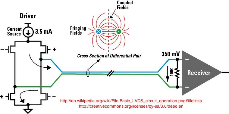
LVDS offers substantial benefits from the differential mode signaling utilized. However, there are serious limitations with LVDS regarding pulsed EMI such as ESD and EFT.

I have noticed a trend of problems with systems using LVDS over the last several years. The problems result from the approximately two Volt common mode range of LVDS. Once this limit is exceeded, the receiver input saturates and the data is lost. Such a common mode voltage may be generated by ESD and EFT under certain conditions including:
  • Signals that leave the circuit board on which they are generated
  • Signals that travel over long shielded cables (one meter or more, for instance) or over any length of unshielded cables outside of a shielded enclosure
  • Single point grounding is attempted in the system design
  • Some PCB stack-ups and layouts, such as traversing from an upper layer referenced to a ground plane of a board with many layers, for instance 16, to a lower layer referenced to a power plane unless several other conditions are met
  • The signals are generated or used on a four layer PCB, unless great care is taken in routing and grounding
If the receiver is likely to be driven into saturation by any cause, it is necessary for the system to be tolerant of the errors that will be generated in the data. If not, the system will likely experience problems, especially when ESD and/or EFT is present either for an intended test or in the operating environment of the equipment. Meeting one or more of the conditions above does not guarantee a problem, but there is a substantial risk of serious system problems if the system is not error tolerant. A good rule of thumb for LVDS is to consider it as two unbalanced signals with no common mode rejection as far as pulsed EMI from sources like ESD and EFT are concerned.

Summary: Differential signaling, such as LVDS, does not necessarily confer immunity to EMI generated by pulsed sources like ESD and EFT. In fact, problems are likely to occur under a set of PCB, cable, and enclosure conditions that occur in many systems.

Check out my public seminar offering in Boulder City, NV. This is one of the best seminar values around because the industry typical fee includes more than just the seminar and lunch, but airport transportation in NV, lodging in the historic Boulder City Dam Hotel and Museum, and breakfast and lunch each day. Click here for more details.

If you like the information in this article and others on this website, much more information is available in my courses. Click here to see a listing of upcoming courses on design, measurement, and troubleshooting of chips, circuits, and systems. Click here to see upcoming seminars in Boulder City, NV.

Boulder Dam Hotel and Museum
Our office, laboratory, and classrooms are located in the
----------
Historic Boulder City Dam Hotel and Museum
1305 Arizona Street, Boulder City, Nevada 89005
Phone: (702) 293-3510
----------
Come for a technical seminar, design review/troubleshooting, or just for a visit and mix a little history of the Old West with your work!


Hangar One
Our Silicon Valley associate office and lab are located at
----------
NASA-Ames Research Center
RMV Technology Group
Bldg. 19, Suite 1073, M/S 19-46C
Moffett Field, CA  94035


Is your product failing ESD testing? Attend my webinar on sources of error in ESD testing. This webinar covers problems and mistakes often made in testing products for ESD compliance that can cause a good product to fail when it should pass. The webinar is given as both a scheduled event and on-demand. Contact me at doug@dsmith.org for more details. Don't let your product fail ESD testing unnecessarily. This webinar is an easy, cost effective solution.
Need help with a design or additional training on technical subjects? Click on the image below to go to CircuitAdvisor.com, a new engineering resource for training, news, and fun.

CircuitAdvisor.com


Click here for a description of my latest seminar titled (now also available online as a WebEx seminar):

EMC Lab Techniques for Designers
(How to find EMC problems and have some confidence your system will pass EMC testing while it is still in your lab).


Top of page
Home

Questions or suggestions? Contact me at doug@dsmith.org
Copyright © 2013 Douglas C. Smith