Crossing Ground Plane Breaks - Part 2
Tracing Current Paths
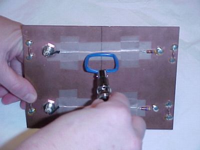
Figure 1. Test Board with Square Loop Positioned for Measurement

Address: P. O. Box 1457, Los Gatos,CA 95031
TEL: 800-323-3956/408-356-4186
FAX: 408-358-3799
Mobile: 408-858-4528
URL: www.dsmith.org
Email: doug@dsmith.org
Figure 1. Test Board with Square Loop Positioned for Measurement
Abstract: EMC and signal integrity engineers know that a signal crossing overa break in a ground plane often causes reflections as well as immunity andEMC problems. Inthis Technical Tidbit, a method is shown to determine where signal currentsflow when a signal path crosses a break in a ground plane. Scope waveformsare included to show typical results. The results clearly show the loop(antenna) that is formed by the signal and its return path in the groundplane.
Discussion: Figure 1 above shows a test board with two paths, bothrun about 12 cm from a BNC connector to a 47 Ohm load over a ground plane.One path stays over the solid ground plane while the other path crosses a5 cm cut in the ground plane. This board simulates a 4 layer board with cutsin both the power and ground planes. The path crossing the break in the groundplane will be of primary interest for this Technical Tidbit article. Theshort wire loops soldered to the ground plane on the left and right sidesare for measuring ground plane voltage in another experiment and are notused for this article.
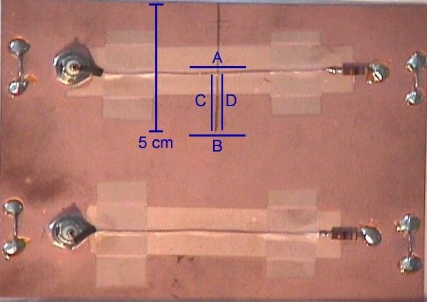
Figure 3 shows the loop output at position A. The loop output is thederivative of the signal current (M di/dt), but it can be used to sense wherethe current is flowing and its direction. The signal source is a square wavefrom the 5-50 MHz oscillatordescribed on this site. The positive and negative going peaks correspondto the edges of the square wave. The edges of the square wave are a little"softer" or rounder than the oscillator would normally have because of theheavy load presented by the 47 Ohm resistor. The scope is triggered directlyfrom the oscillator so the relative directions of the edges of the waveformcan be compared.
When the loop is moved to position B with the same orientation, the plotin Figure 4 results. Notice that it is inverted from Figure 3. Thismeans that the current is flowing in the opposite direction around the endof the ground break. The amplitude is a little smaller in Figure 4 likelybecause the current is not parallel to the loop for its full length (it bendsaround the end of the break) and the lower inductance of the ground planecompared to the signal wire.
| 10 mV/div | 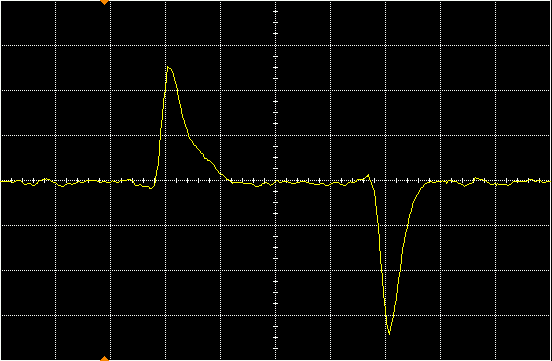 | ||
| 10 ns/div | |||
| Figure 3. Loop Voltage (Position A) | |||
| 10 mV/Div | 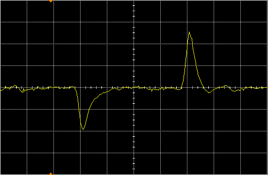 | ||
| 10 ns/div | |||
| Figure 4. Loop Output Voltage (Position B) | |||
Figures 5 and 6 show the loop output at positions C and D respectivelywith the loop held in the same orientation and just slid from C to D. Noteagain the reversed current directions indicating the current is flowing downone side of the break and up the other. If a smaller loop (for better resolution)was scanned over the board, one could trace out the complete signal pathfrom the source to the load and back to the source again.
| 10 mV/Div | 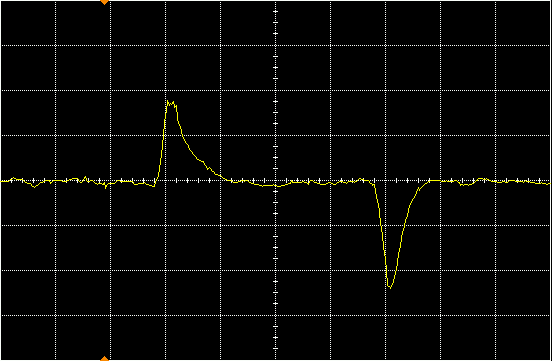 | ||
| 10 ns/div | |||
| Figure 5. Loop Output Voltage (Position C) | |||
| 10 mV/Div | 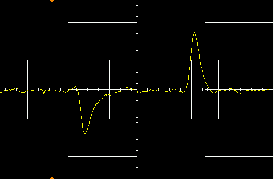 | ||
| 10 ns/div | |||
| Figure 6. Loop Output Voltage (Position D) | |||
One can see from the data above that the signal return current flowingin the ground plane is diverted to the end of the break and thus forms asubstantial loop area with the signal path for the signal current. This largeloop has many implications for system operation including being more susceptible to external EMI (electromagnetic interference).
For related information pertaining to magnetic loops on this website see:
The waveforms in this article were taken with an AgilentInfinium 54845a oscilloscope.